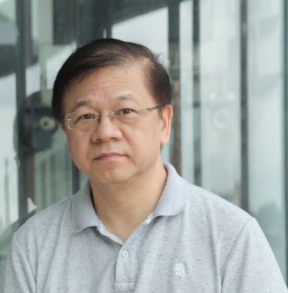
Faculty
Wei-I Lee
Professor
Ph.D. in Electrical Engineering , Rensselaer Polytechnic Institute , USA
Office
Science Building III, SC 560
Tel.
(03)5712121#31773
Lab.
Science Building III, SC 706, 756 Ext. 56161
Biography
Experience
Expertise
Publications
1981
B.S., Department of Electrophysics, Natl. Chiao Tung U.
1985
M.S., Electrical Engineering, U. of Wisconsin-Madison.
1988
Ph.D., Electrical Engineering, Rensselaer Polytechnic Institute, USA
2021/02 -
Professor, Department of Electrophysics, Natl. Yang Ming Chiao Tung U.
1997/08 - 2021/01
Professor, Department of Electrophysics, Natl. Chiao Tung U.
1991/08 - 1997/07
Associate Prof., Department of Electrophysics, Natl. Chiao Tung U.
1988 - 1991
Engineer, Varian Associates Research Center
  1. Optoelectronic Semiconductor Devices and Physics
  2. Semiconductor Nano-structures.
  1. Yin-Hao Wu, Chuo-Han Lee, Chung-Ming Chu, Yen-Hsien Yeh, Chan-Lin Chen, and Wei-I Lee (2013, Aug). A Simple Growth Method to Produce a-Plane GaN Thick Films by Hydride Vapor Phase Epitaxy. Japanese Journal of Applied Physics, (52) 08JB08.
  2. Yen-Hsien Yeh, Kuei-Ming Chen, Yin-Hao Wu, Ying-Chia Hsu, Tzu-Yi Yu, and Wei-I Lee (2011, Oct). Hydrogen etching of GaN and its application to produce free-standing GaN thick films. J. Cryst. Growth, 333 (2011) 16–19. NSC 99- 2119-M-009-005-MY3.
  3. Kuei-Ming Chen, Yin-Hao Wu, Yen-Hsien Yeh, Chen-Hao Chiang, Kuei-You Chen, and Wei-I Lee (2011, Mar). Homoepitaxy on GaN substrate with various treatments by metalorganic vapor phase epitaxy. J. Cryst. Growth, 318 (2011) 454–459. NSC 98-2221-E-009-026.
  4. C.H. Chiang, K.M. Chen, Y.H. Wu, Y.S. Yeh, W.I. Lee, J.F. Chen, K.L. Lin, Y.L. Hsiao, W.C. Huang, and E.Y. Chang (2011, Jan). Nonpolar a-plane GaN grown on r-plane sapphire using multilayer AlN buffer bymetalorganic chemical vapor deposition. Appl. Surf. Lett., 257 (2011) 2415–2418. NSC 96-2112-M-009-034- MY3.
  5. Yen-Hsien Yeh, Kuei-Ming Chen, Yin-HaoWu, Ying-Chia Hsu and Wei-I Lee (2011, Jan). Hydrogen etching on the surface of GaN for producing patterned structures. J. Cryst. Growth, 314 (2011) 9–12. NSC 99-2119-M-009-005-MY3.
  6. Kuei-Ming Chen, Yen-Hsien Yeh, Yin-Hao Wu, Chen-Hao Chiang, Din-Ru Yang, Chu-Li Chao,Tung-Wei Chi, Yen-Hsang Fang, Jenq-Dar Tsay, Wei-I Lee (2010, Dec). Method for Modulating the Wafer Bow of Free-standing GaN Substrates via Inductively Coupled Plasma Etching. J. Cryst. Growth, 312 (2010) 3574– 3578. NSC 98-2221-E-009-026.
  7. Kuei-Ming Chen, Yen-Hsien Yeh, Yin-Hao Wu, Chen-Hao Chiang, Din-Ru Yang, Zhong-Shan Gao, Chu-Li Chao, Tung-Wei Chi, Yen-Hsang Fang, Jenq-Dar Tsay, and Wei-I Lee (2010, Sep). Stress and Defect Distribution of Thick GaN Film Homoepitaxially Regrown on Free-Standing GaN by Hydride Vapor Phase Epitaxy. Jpn. J. Appl. Phys, 49 (2010) 091001. NSC 98-2221-E-009-026.
  8. Kuei-Ming Chen, Hsin-Hsiung Huang, Yi-Lin Kuo, Pei-Lun Wu, Ting-Li Chu,Hung-Wei Yu, and Wei-I Lee (2009, May). Effective reduction of bowing in free- standing GaN by N-face regrowth with hydride vapor-phase epitaxy. J. Cryst. Growth, 311 (2009) 3037–3039. NSC 95-2662-E-009-011.
  9. Hsin-Hsiung Huang*, Chu-Li Chao, Tung-Wei Chi, Yu-Lin Chang, Po-Chun Liu,Li-Wei Tu, Jenq-Dar Tsay, Hao-Chung Kuo, Shun-Jen Cheng*, Wei-I Lee (2009, Jan). Strain-reduced GaN thick-film grown by hydride vapor phase epitaxy utilizing dot air-bridged structure. J. Cryst. Growth , 311 (2009) 3029– 3032. (SCI). NSC 97-2622-E-009-002.